Designing a RISC-V CPU, Part 2: Successfully executing (some) instructions
Mon 01 March 2021The previous instalment of this series was "basically an explanation of what FPGAs are and a 'hello world' nMigen example."1 In this post, I will be detailing the design of my CPU as it currently stands, and going over the various mistakes I made along the way. As with the previous post, I am primarily aiming this at software engineers who are new to hardware design – but I hope it will be interesting to anyone interested in nMigen, RISC-V, or CPU design generally.
I hope the mistakes I made along the way will be a useful frame for considering these questions:
-
What about digital logic design is fundamentally different from software design?
-
What about digital logic design is similar to software design?
You can see the code for my CPU at the time of writing here or an up to date version here.
An introduction to RISC-V
RISC-V ("risk five") is an open standard instruction set architecture (ISA). "RISC" means "reduced instruction set computer", broadly meaning that the ISA prioritises simple instructions. In contrast, CISC (complex instruction set computer) ISAs are optimised to perform actions in as few instructions as possible, hence their instructions are often more complex. ARM architectures are RISC; x86-related architectures are CISC.
Usually in industry, ISAs are patented, so in order to implement the ISA you need an (expensive) license from the vendor. Often, commercial ISAs are poorly documented, with the motivation behind design details not always being available even after such a license agreement.
From the RISC-V spec 2:
Our goals in defining RISC-V include:
- A completely open ISA that is freely available to academia and industry
- a real ISA suitable for direct native hardware implementation, not just simulation or binary translation.
- An ISA that avoids "over-architecting" for a particular microarchitecture style, but which allows efficient implementation in any of these.
Additionally, a lot of commercial architectures are complex and burdened with backwards-compatibility constraints. RISC-V offers a fresh start!
The ISA doesn't explain the details of how to design a CPU – it just defines an abstract model of the CPU, mostly by defining what instructions the CPU must support, including:
- The encoding of the instructions (i.e. how to construct the machine code that the CPU will run)
- The registers (the very fast, very small storage locations accessed directly by the CPU)3
How to actually create a CPU that realises these requirements is up to us \o/
A quick note (feel free to skip if you don't have opinions about CPUs)
I'm trying to design a single-stage CPU; that is, I'm trying to design a CPU that retires one instruction per clock cycle with no pipelining. Usually CPUs have pipelining in place to maximise efficiency. I am hoping that avoiding this will result in a simpler design more suitable to my learning. Perhaps it will complicate other aspects of the design (like my program counter having 3 outputs), but I'm certainly finding it easier to hold the design in my head when I only have to think about this clock cycle and the next. I will likely discuss this in more detail in the next blog post where I implement the load instructions. I have a plan for how to make these work in a single cycle, but they do pose a particular challenge and I may change my design as a consequence.
Designing a CPU
RISC-V defines various ISA modules; I will be implementing RV32I, the base 32-bit integer instruction set.
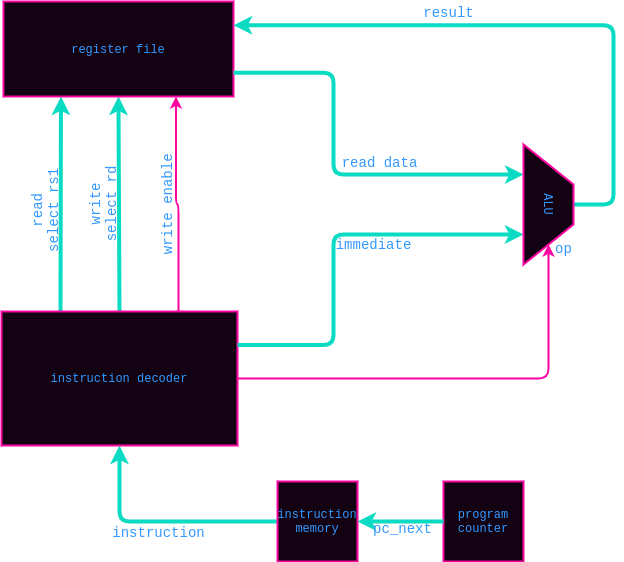
To design my CPU, I first looked at the JAL (jump and link) and the ADDI (add immediate) instructions, and drew a block diagram of what hardware would be needed to decode those instructions. I think the ADDI instruction is easier to grasp if you're not used to thinking about how machine code is encoded, so we'll start with that. If this all totally foreign to you, you might enjoy my introduction to ARM assembly.
Decoding ADDI

ADDI adds the sign-extended 12-bit immediate to register rs1
Let's break some of this down, imagining we're decoding such an instruction:
- An immediate is analogous to a literal value in source code; the value itself is encoded in the instruction, rather than e.g. retrieved from a register.
- The opcode field is the same value for all the instructions listed here.
- Once we've read the opcode, we know that bits 12-14 contain the funct3 field (3 for 3 bits), which encodes whether this is an ADDI instruction (or SLTI, ANDI &c.)
So, somehow we will have to:
- Retrieve the value stored in register rs1
- Therefore, our register file needs an input for selecting this register to read, and an output for the data read from that register.
- Add that to the immediate value
- An arithmetic logic unit (ALU) will be helpful
- Store the result in register rd
- Our register file also needs write select and write data inputs.
Sign-extension will be necessary too – this is just the process of taking a number narrower than (in our case) 32 bits, and filling in the remaining bits such that two's complement arithmetic will be performed correctly. I won't include this in the diagram below.
Implicit in all this is that we'll need some way to retrieve the instruction itself and pass it to the instruction decoder. The program counter is what tells the instruction memory which address to retrieve an instruction from.

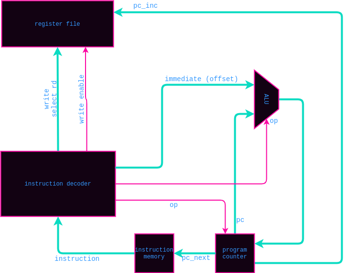
I'm using thick cyan lines for data flow and thin magenta lines for control flow.
JAL
Now let's try doing the same for JAL.
The jump and link (JAL) instruction [...] immediate encodes a signed offset in multiples of 2 bytes. The offset is sign-extended and added to the
pcto form the jump target address. [...] JAL stores the address of the instruction following the jump (pc+ 4) into register rd.
There's a lot more going on here, particularly if you aren't familiar with machine code. We noted above that the program counter sets which instruction will be executed next. Usually the program counter simply increments to the next address each cycle – that's how we continue to execute our program! However, say our program calls a subroutine stored elsewhere in memory; we'd need a way to jump to the subroutine address. Or, say we wanted an infinite loop (ubiquitous in embedded software!); we'd need a way to jump4 back to the address at the start of the loop. JAL allows for these situations.
The "link" part of JAL is the part where the next instruction is stored in the destination register. This is convenient when the jump is used to execute a subroutine: once the subroutine completes, we can jump back to that stored instruction address.
Here's the encoding for JAL:

Note:
- The opcode uniquely defines the JAL instruction (no other instructions share this opcode)
- We need to unshuffle the immediate to get the offset
- The LSB5 of the immediate is not encoded because it must be 0: only offsets in multiples of 2 bytes are supported.
The unshuffling caused me some pain in my code, so it's amusing to me that it won't be part of the block diagram below. But it's part of the internals of the instruction decoder, not its interface, which is what we are determining with these diagrams. The shuffled bits might seem nonsensical, but they're chosen to maximise overlap with other instruction formats in RISC-V.

Putting ADDI and JAL together
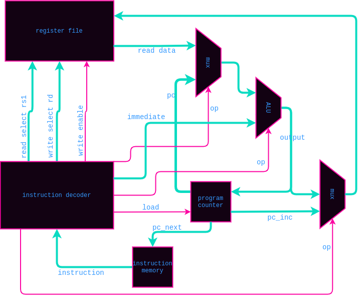
The next challenge is to draw a block diagram that implements both ADDI and JAL. The first obvious problem: the inputs to the ALU are different in both cases, as is the wiring of the output. We need some kind of logic block that can pick between them depending on some control signal: a multiplexer (mux).
We also need a way to tell the program counter whether the next instruction address should come from a set address or from incrementing the current address.
Here's what my design looks like at the moment (excluding a few things I have because I know I'll need them later, like two read select/data signals on the register file):

Implementing the design
As covered in my previous blog post, I'm using nMigen to implement my design. As I'm currently designing a single-stage CPU, more of my design is combinatorial, rather than synchronous, because I don't require the additional state that pipelining necessitates. This most likely means my design is unable to run quickly, but that's not a concern of mine.
I don't think it's helpful to post all the source code of my implementation in this blog, but I will include some code here to illustrate mistakes that I made and what I learned from them.
Mistake #1: thinking about my logic circuit sequentially
I initially implemented my program counter incorrectly after I got really
confused about when synchronous updates would take effect. I initially only had
the pc and pc_inc outputs because I didn't really understand the difference
between pc and pc_next. It's taken some getting used to thinking about the
whole logic circuit "happening at once"7, rather thinking sequentially like
I would when writing software. This is what led to my confusion. Properly
conceptualising your circuit in this way is key, and a challenge if you're used
to writing software.
 1 """Program Counter"""
 2 import nmigen as nm
 3
 4 INSTR_BYTES = 4
 5
 6
 7 class ProgramCounter(nm.Elaboratable):
 8     """
 9     Program Counter
10
11     * load (in): low to increment, high to load an address
12     * input_address (in): the input used when loading an address
13
14     * pc (out): the address of the instruction being executed this clock cycle
15     * pc_next (out): the address of the instruction being executed next clock
16       cycle
17     * pc_inc (out): the address after that of the instruction being executed
18       this clock cycle
19     """
20
21     def __init__(self, width=32):
22         self.load = nm.Signal()
23         self.input_address = nm.Signal(width)
24         self.pc = nm.Signal(width)
25         self.pc_next = nm.Signal(width)
26         self.pc_inc = nm.Signal(width)
27
28     def elaborate(self, _):
29         m = nm.Module()
30
31         m.d.comb += self.pc_inc.eq(self.pc + INSTR_BYTES)
32         m.d.sync += self.pc.eq(self.pc_next)
33
34         with m.If(self.load):
35             m.d.comb += self.pc_next.eq(self.input_address)
36         with m.Else():
37             m.d.comb += self.pc_next.eq(self.pc_inc)
38
39         return m
When thinking about my implementation, I now want to answer these questions:
- What is my state?
- How are the outputs computed?
- How is the state updated?
This sounds simple, but it has been clarifying. For this case:
pcis my state (you'll note it is assigned synchronously, so its value is updated at the start of the next clock cycle).pc,pc_inc, andpc_nextare the outputs:- the
pcoutput is the current state pc_incis justpc + 4pc_nextswaps betweenpc_incand theinput_addressbased on load
- the
- Each clock cycle,
pctakes on the value ofpc_next
Mistake #2: Creating a combinatorial loop
This isn't really an additional mistake, as the incorrect program counter implementation described above caused this. I felt this particular consequence deserved its own subsection.
When I only had the pc and pc_inc outputs from my program counter, I
created the following combinatorial loop:
- the
pcoutput was an input to the ALU - but the
pcoutput was computed from the output of the ALU
Both of these signals were in the combinatorial domain, so they were effectively wired together in a loop.
The creation of this feedback loop resulted in my tests hanging as my combinatorial simulations never settled. If I'd tried to synthesise my design, the synthesis tools would have refused. If you were able to synthesise such a design, the output would be constantly changing.
Mistake #3: Not creating the block diagram correctly
True Fans™ of this blog might notice that the block diagram above has a notable difference from the one shown at the end of the previous blog post: previously I didn't mux the input of the ALU. I was wondering why JAL wasn't working, and tried to trace it through my block diagram, like we did above. A re-enactment:
Computer, show my original sketch of the block diagram.

Computer, enhance:

Me:

The above is a bit frivolous, but I'd say the lesson here is to think actively about your block diagram (or whatever reference you are using while implementing your design), making sure it actually makes sense to you and does what you want it to. This applies to software design too when viewing any requirements or other design documentation, of course.
Miscellaneous mistakes
I made a lot of other mistakes that aren't that interesting to cover – most notably really messing up the unshuffling of the immediate in the JAL instruction. But that was just a programming error without an interesting lesson to be learnt from it.
Running my first program!
It was a very exciting moment when I figured out the last of the mistakes I had made in my implementation, with the help of my tests and of gtkwave.
For convenience in tests, my instruction decoding code also has code for assembling instructions. I use it here to create a simple program with two instructions:
-
An
ADDIinstruction whererdandrs1are the same register, and the immediate is1. This means it will increment the value inrs1. -
A
JALinstruction with an offset of -4, meaning it jumps back to ourADDIinstruction. This creates an infinite loop where the value in a register is incremented each clock cycle.
The LED code is specific to my board. I'm selecting 4 bits (one for each LED) in the register and displaying them on the board's LEDs. I pick bits in the middle so they don't change too quickly to see (as would be the case if I picked the LSBs) or too slow to look cool (as would be the case if I picked the MSBs).
 1         program = [encoding.IType.encode(
 2                         1,
 3                         reg,
 4                         encoding.IntRegImmFunct.ADDI,
 5                         reg,
 6                         encoding.Opcode.OP_IMM),
 7                    # jump back to the previous instruction for infinite loop
 8                    encoding.JType.encode(0x1ffffc, link_reg)]
 9
10         imem = nm.Memory(width=32, depth=256, init=program)
11         imem_rp = m.submodules.imem_rp = imem.read_port()
12         m.d.comb += [
13                 imem_rp.addr.eq(cpu_inst.imem_addr),
14                 cpu_inst.imem_data.eq(imem_rp.data),
15         ]
16
17         colours = ["b", "g", "o", "r"]
18         leds = nm.Cat(platform.request(f"led_{c}") for c in colours)
19         m.d.sync += leds.eq(cpu_inst.debug_out[13:17])
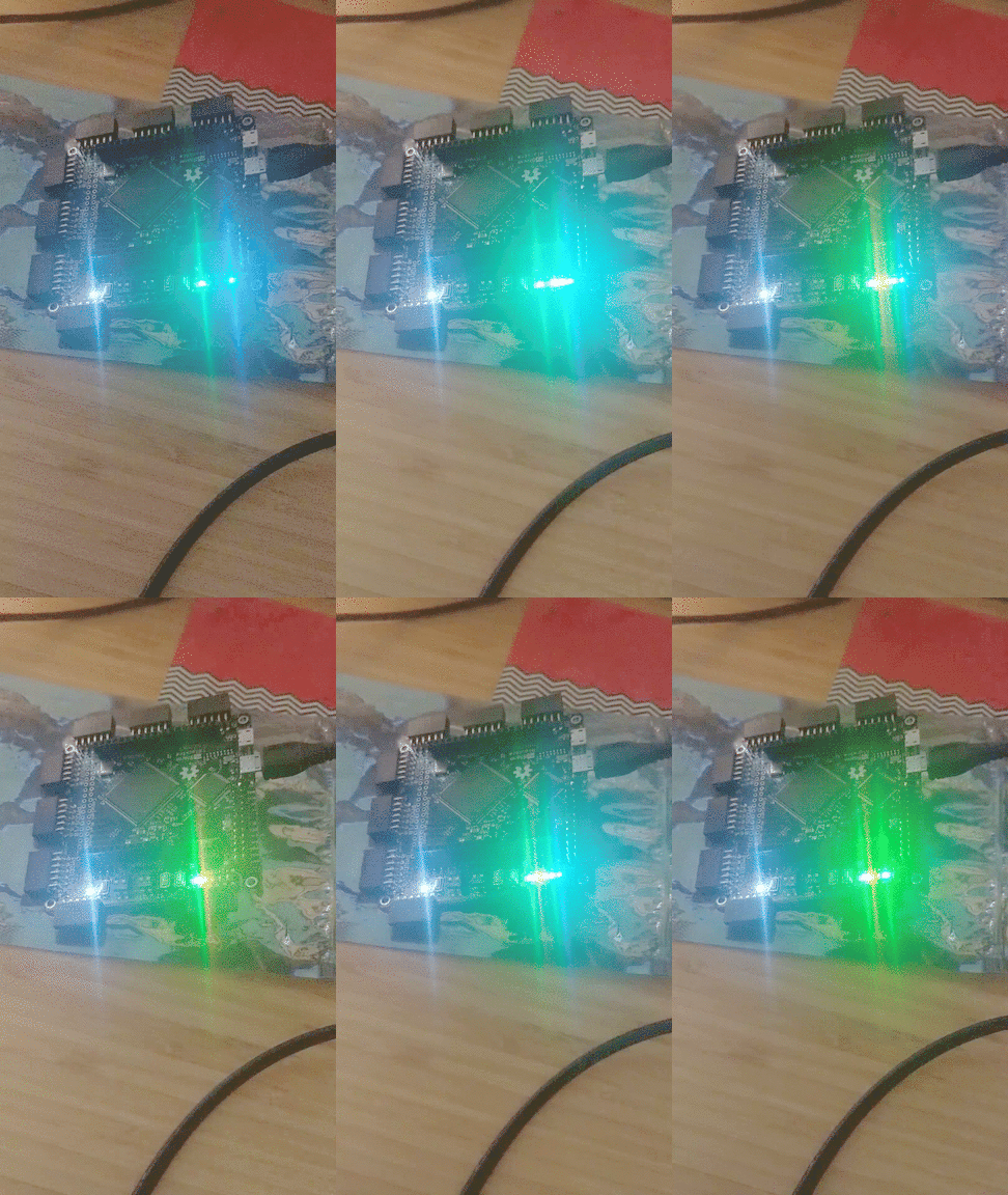
And here is a poor quality gif of the LEDs! Very exciting.

The next stage will be to implement the rest of the RV32I instructions. Probably I will start with the load instructions, as I think they will pose a challenge in my current single-stage architecture. I have a plan for how to address that. If you'd like to see future instalments of this blog series, you can follow me on Twitter or subscribe to my RSS feed.
Differences and commonalities between software design and digital logic design
Now that I've completed a lot more of the design and implementation of my CPU, I have some clearer thoughts on this topic. I thought there would be some clear differences in kind between software design and digital logic design. After much thought, I wonder if there are merely differences in degree.
Concurrency
First, let's consider concurrency. This is a topic that's sometimes misunderstood, so let's be clear: concurrency happens whenever different parts of your system might execute at different times or out of order6. A system is concurrent if it can support having multiple tasks in progress at the same time; this could be in parallel, or it could involve switching between the tasks while only actually executing one at any given moment.
Arguably, the default state for software is to have no concurrency – it often needs explicitly created (e.g. by creating a thread), or at the very least, it needs explicitly handled (e.g. in an interrupt handler). I think any software engineer who has worked on concurrent software would agree that dealing with concurrency is a singular challenge that creates room for difficult and subtle bugs. For these two reasons, software generally has limited concurrency.
Now imagine concurrency is your default state, and that every single piece of state is updating all at once every step of your program.
That is the default state of digital logic. While in software you generally have to explicitly create (or at least explicitly handle) concurrency, in hardware you have to deliberately make something sequential.
I said above that concurrency in software is challenging. If digital hardware has more concurrency, is it more challenging to design? Perhaps! It's hard for me to comment on this due to my lack of experience in hardware design.
Perhaps one reason that concurrency is so difficult in software is the annoying habit of a lot of software8 to be dependent on a colossal amount of state. How many possible states does a mere kilo-bit of memory have? 2^{1024} is too big a number for me to conceptualise. And yet a kilo-bit is nothing by many program's standards.
In hardware, state is more precious. My FPGA is only so large. I have an
ice40hx8k, which has 8000 logic cells. Each cell has one 4-input LUT and one
flip-flop: so let's say 8000 bits of state. Pathetic! Watch me create
millions of bits of pure chaos with a single call to malloc.
And of course, if you were designing for silicon, the size of your design would be directly related to cost!
Verification
So, we've considered concurrency. Another thing I wondered is whether digital hardware has some fundamental property that makes it easier to formally verify, or at least to demonstrate equivalence with a model. When I worked on a system that could kill people if it malfunctioned, in our risk assessments we had to assume 100% chance of software failure. Practically this generally meant that software mitigation alone was not enough. I found it strange that the FPGA component of our system was considered much more trusted. Did hardware have some fundamental property that made it "better"?
Once again, I don't think there is a fundamental difference here. After all, software exists that has been formally verified. In general, functional programming lends itself better to this due to the separation of state and behaviour. It seems more likely that the difference is in the careful management of state. The properties of digital hardware described above encourage this, but it's not impossible to do in software.
The huge teams of verification engineers that work on silicon design might also suggest some fundamental difference, given you might not have seen the same applied to software. However, there are software projects that are given this level of rigour! Most famously, much of NASA's software, like software for space shuttles9. The sad truth is that most companies don't consider it worth it to apply this rigour to their software (it's hugely expensive!). When sufficient lives and/or money are on the line, software can and is written and tested with the same level of rigour as a lot of hardware..
If you have thoughts to share on what you think the differences and commonalities between hardware and software design are, please share them via email or in Hacker News comments if you have come from there. It's been really interesting to ponder, and I'd be interested in different perspectives.
-
Hacker News comment, 2021 ↩
-
https://riscv.org/wp-content/uploads/2017/05/riscv-spec-v2.2.pdf ↩
-
Just a note: the word "register" is pretty overloaded. You may have heard it in the context used above (the small storage accessed directly by the CPU); for memory-mapped IO in a microcontroller; you may have also heard "register" used as a verb to describe saving state in hardware. ↩
-
I think generally "branch" is used to describe conditional instructions, whereas "jump" is used to describe unconditional instructions. Certainly this is the case in RISC-V, but I think it very much depends on the particular architecture, and sometimes they are used interchangeably. ↩
-
Least Significant Bit ↩
-
wording from https://docs.rust-embedded.org/book/concurrency/ ↩
-
Of course in analogue reality things are not happening at exactly the same time, but our abstraction is the discrete time period of our clock. ↩
-
functional programmers, we don't need your smugness here! ↩
